Keyboard interface in VHDL
This design consists of 4 modules to interface an FPGA with PS2 keyboard using DE2-115 (the same code can be used with any FPGA board)....


32-bit ALU in VHDL
In this post the design of a 32-bit ALU will be presented. The ALU has 2 data inputs A & B, 1 carry input and ALU control input....


Xilinx XADC Part 1 : Analog input
Introduction The XADC is available on the Xilinx 7 series FPGA's, it includes a12-bit, 1 Mega sample per second (MSPS) ADC and...


Xilinx XADC Part2 : Multiple analog inputs
In this project the Xilinx XADC will be used to sample 3 external analog input signals for this purpose the XADC will be configured to...


Full Adder in Verilog
The Full Adder circuit performs the addition of two input bits A & B and and input carry, and the result is the sum S and a carry out....


Xilinx XADC Part3 : Internal temperature sensor
The XADC contains a number of sensors in addition to the analog input channels, these sensors are the power supply sensors and the...


Encoder design in Verilog
In digital circuits, the encoder is a component that performs one hot to binary conversion, That is, if there are 2^n input lines, and at...


Decoder design in Verilog
Decoder is one of the main combinational components in digital circuits that converts binary information from the n coded inputs to a...


Multiplexer design in Verilog
The multiplexer is an essential digital circuit to select one of different inputs, we are going to illustrate the different methods of...
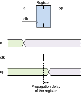
Flip Flops & Latches in Verilog
D Flip-Flops & Latches are the smallest storage elements in digital circuits. the D-flip flop stores the value of input D with the rising...